Semiconductor UV Series Filters
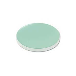
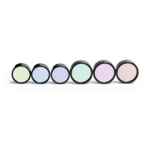
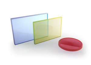
The semiconductor ultraviolet filter is a multi-layer hard film TFF interference thin film filter, specially developed for wafer inspection, photolithography, thin film measurement, and semiconductor fluorescence defect detection. It is divided into three categories according to the ultraviolet band:
1. Deep UV DUV (185-300nm): 193nm (ArF), 248nm (KrF), 266nm, 280nm, photolithography, deep UV defect detection
2. Middle ultraviolet UVB (300-360nm): 313nm, 340nm, thin film thickness spectral detection
3. Near ultraviolet UVA (360-40nm): 365nm (i-line lithography), 405nm (g-line), mainstream optical path for mass production machines
Four mainstream categories&corresponding applications of semiconductors
1. UV narrowband bandpass filter BP-UV
Core function: Only passing through a single ultraviolet wavelength of the target, blocking stray light and laser plasma interference across the entire wavelength range, and improving the signal-to-noise ratio of defect imaging
Lithography equipment: 365nm i-line, 405nm g-line alignment optical path, uniform illumination
Wafer inspection: 280nm deep ultraviolet defect scanning, 340nm film thickness measurement
Laser measurement: 193/266nm ultraviolet laser reflection/scattering detection
2. Ultraviolet long/short wave pass filter LWP/SWP
LWP Long Wave Pass: Cut off short wave DUV, transmit target UV+visible light, separate excitation light from fluorescence receiving path
SWP Short Wave Pass: Cut off visible and infrared light, only transmit ultraviolet light, filter white light impurities at the light source end
Combined with a dichroic mirror to form a confocal ultraviolet detection optical path
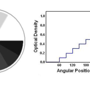
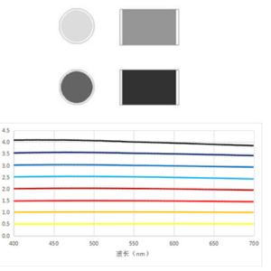
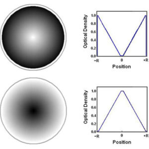
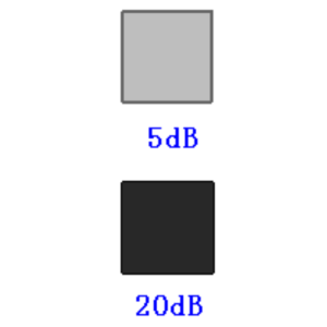
3. UV neutral density ND attenuation film (variable density/fixed OD)
Balance UV laser power to prevent CCD/PD detector saturation
Multi channel wafer inspection machine unifies the UV light intensity of each channel to eliminate channel differences
Band neutrality: uniform attenuation of 190-400nm, no wavelength selectivity
4. UV notch filter Notch
Suppress the fundamental wave of strong ultraviolet laser and only transmit weak defect scattering signals for high-resolution dark field detection
Matching models for semiconductor segmentation scenarios
1. DUV deep ultraviolet lithography/measurement (193/248/266nm)
Model examples: BP193-15, BP248-10, BP266-5
• Supporting substrate: JGS1 UV grade quartz
• Operating conditions: vacuum chamber, excimer laser, ultra-high stray light suppression OD6
2. 365nm i-line lithography, wafer macroscopic defect detection
• Model: BP365-10, LWP380 long pass piece
• Base: JGS2 quartz
• Purpose: Photolithography machine alignment, UV imaging of silicon wafer surface particles/scratches
3. Spectral detection of film thickness (340nm)
Model: BP340-8 Narrowband Filter
Advantages: Narrow bandwidth eliminates multi-stage reflection interference, and the measurement accuracy of thin film thickness is nanometer level
4. 280nm deep ultraviolet micro defect scanning (advanced process 7nm/3nm)
BP280-3 ultra narrowband filter, OD6 deep cutoff, captures submicron defect fluorescence signals
5. UV power balance ND attenuator
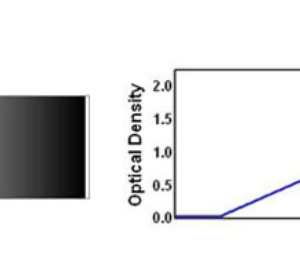
UV ND fixed OD0.1~OD4, linear variable density gradient plate, JGS1 quartz substrate
Core optical parameters (semiconductor industry standard)
1. Spectral core indicators
Parameters Deep UV DUV (< 300nm) Near UV 365/405nm Mass production models
Center wavelength CWL tolerance ± 0.5nm (high-precision lithography ± 0.2nm) ± 1nm
Half width at half maximum (FWHM) 1-5 nm (ultra-high resolution)/10 nm 5-15 nm
Peak transmittance Tmax ≥ 60% (193nm ≥ 12%) ≥ 85%
Cut off depth OD OD5~OD6 (out of band transmittance ≤ 0.0001%) OD4~OD5
Cut off range 180-1100nm, full band depth cut-off 200-1100nm
Edge steepness ≤ 1nm/OD, distinguishing adjacent UV spectral lines ≤ 2nm/OD
PDL polarization loss<0.05dB (forced by laser path)<0.1dB
2. Substrate material selection (semiconductor hard distinction)
1. JGS1 high-purity fused silica (the only DUV deep UV substrate)
High transmittance from 185nm, no impurity absorption, low thermal expansion CTE=0.55e ⁻⁶/K, high temperature resistance, high LIDT; 193/248/266nm must be used
2. JGS2 standard quartz
Transparent above 220nm, universal for mass production testing at 340/365nm, with better cost-effectiveness than JGS1
3. Disable D263T/BK7/K9 glass
Significant absorption of ultraviolet light below 320nm, complete failure of deep ultraviolet light path; Only low-cost and simple devices above 405nm can be temporarily used
There are some stock models available for selection above, if you need custom Optical Semiconductor UV Filters or bulk orders, please contact our sales team:
info@borisuns.com
Related Products